
This article is based on the video titled “How do Electron Microscopes Work? Taking Pictures of Atoms” by Branch Education. Electron microscopes have revolutionized our understanding of the nanoscopic world, enabling us to visualize structures as small as individual atoms. The video delves into the mechanics, applications, and limitations of two main types of electron microscopes: the Transmission Electron Microscope (TEM) and the Scanning Electron Microscope (SEM).
Contents
- The Nanoscopic World and Electron Microscopy
- Types of Electron Microscopes: TEM vs SEM
- The Mechanics of TEM: From Electron Generation to Imaging
- Why Not Just Use Light?
- SEM: Surface Imaging and Limitations
- The Video
The Nanoscopic World and Electron Microscopy
Electron microscopes have been instrumental in the development of nanotechnology, allowing us to visualize and understand structures at the atomic level. They can magnify objects millions of times, far surpassing the capabilities of light microscopes. For example, while light microscopes can only magnify up to 2000 times, electron microscopes can achieve meaningful magnifications up to 2 million times. This is crucial for fields like semiconductor manufacturing, where the ability to see at the nanoscale is indispensable (and yes, this is the same technology that allows us to have increasingly powerful computer chips).
Types of Electron Microscopes: TEM vs SEM
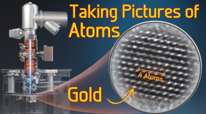
The video explains that there are two main types of electron microscopes: TEM and SEM. TEMs are used for capturing images of structures inside materials, much like how X-rays capture images of bones inside our bodies. SEMs, on the other hand, are used for surface imaging. TEMs are generally more complex and can achieve a resolution up to 50 picometers, which is roughly the size of a hydrogen atom. SEMs have a maximum resolution of around one nanometer. Both types of microscopes have their specific applications and limitations, and the choice between them depends on the research requirements.
The Mechanics of TEM: From Electron Generation to Imaging
Transmission Electron Microscopes operate by generating a beam of electrons, accelerating them to nearly 70% the speed of light, and then focusing these electrons through a specimen. The electrons are scattered as they pass through the specimen, creating an image that is then magnified and captured. The microscope uses a series of magnetic lenses to focus the electrons, and the final image is captured by a high-resolution camera sensor at the bottom of the microscope. The video also discusses the importance of creating a vacuum within the microscope to prevent the scattering of electrons due to air molecules (a fascinating tidbit that underscores the complexity of this technology).
Why Not Just Use Light?
One might wonder why we don’t simply use light for such microscopic observations. The video explains that the wavelength of visible light is much larger than the structures we aim to observe at the nanoscale. Electrons, when accelerated, have a much shorter wavelength, allowing for higher resolution. This is a key advantage of electron microscopes over their light-based counterparts.
SEM: Surface Imaging and Limitations
Scanning Electron Microscopes work by focusing a beam of electrons onto a specimen and scanning it to create an image. Unlike TEMs, which capture images of internal structures, SEMs are used for surface imaging. The resolution of SEMs is limited by the size of the focused electron beam and the depth to which the electrons penetrate the sample. While SEMs are excellent for surface imaging, they are not suitable for internal imaging at the atomic level.
This article does not aim to be a conclusive discussion but rather an informative guide based on the comprehensive video by Branch Education. The video itself is a treasure trove of information for anyone interested in the intricacies of electron microscopy and its impact on modern science and technology.